There are no schematics as such for the big crystal rectifier boards. Their design comes from Verilog-like source files. Those source files are passed to a compiler which then generates PC boards with the gates in place. The connections within each gate are already routed but the connections between the gates are not routed, and so it takes about a whole day to route one of the boards.
Here are the source files:
Note: Variables beginning with _ are active low.
Also, the basic gate using one triode is the AND-OR-INVERT (AOI) gate. So that form is used wherever possible to make most efficient use of tubes (and time), sometimes at the expense of a few extra crystal rectifiers. It takes just as many triodes to make a wide AOI gate as it does an inverter, ie 1. An XOR can be made from 2 triodes (1 AOI + 1 NOR) instead of 4 NANDs. XOR = ~(~(A | B) | A & B).
There is also a source file for the 4 bus connectors, A,B,C,D, and the three power connectors:
To keep timing simple, the design is fully synchronous, ie, the flipflops clock on the positive edge of the clock. The clock comes out of the RasPI and is called clok2. It then goes through an inverter and is called _clok1. Then one more inverter gives it the name clok0 which is the only version that goes to the flipflops so they all clock at the same time. There are several _clok1 and clok2 inverters in parallel for fanout.
To reduce circuitry, there are some cases of gated clocks (the accumulator, link and memory address register). The state flipflops and the program counter flipflops clock every cycle. Like you can see in pc.mod that the T inputs to the DFF modules come directly from the ungated clock. And in ma.mod you can see the T inputs come from a gated clock, gated by a DFF that gets clocked on the negative edge of the clock. A flipflop is used for the gating so as to be glitch-free and is arranged so as to preserve the timing with the non-gated clocking, ie, one inverter from _clok1 through the gated clocks going into the flipflops.
The compiler is a big program called netgen that reads in those module files and produces a PC board and a report file. The report file says where the various gates are located on the board.
So suppose the FETCH2 flipflop is stuck on, OMG. Where are the tubes? So look in seq.mod to find the FETCH2 flipflop:
fetch2: DFF (_PS:_reseta, _PC:1, T:clok0a, D:_fetch2d, Q:_fetch2q, _Q:fetch2q);
And we see it is called fetch2 obviously, and we can see what the input names are and output names.
Now look in seq.rep (as generated by netgen) for fetch2:
    0.DFF/fetch2/seqcirc
     f   Q out: J16    6.9, 5.6  2R-U6A  =>  Q.f.0.DFF/fetch2/seqcirc
                                         =>  D490  16.1,10.1  D_1.0.fetch2qa/seqcirc[0:0]1<1>
                                         =>  D484   5.1, 5.8  D_2.e.0.DFF/fetch2/seqcirc<1>
     e  _Q out: J15    5.9, 5.6  2R-U6B  =>  Q.e.0.DFF/fetch2/seqcirc
                                         =>  D128  12.1,10.8  D2_1.0._alub_m1/seqcirc[0:0]3<1>
                                         =>  D35    5.1, 2.6  D_1.b.0.DLat/ireg09/seqcirc<1>
                                         =>  D22    3.1, 2.6  D_1.b.0.DLat/ireg10/seqcirc<1>
                                         =>  D7     1.1, 2.6  D_1.b.0.DLat/ireg11/seqcirc<1>
                                         =>  D486   6.1, 5.6  D_1.f.0.DFF/fetch2/seqcirc<1>
                                         =>  D33    5.1, 1.3  D_2.a.0.DLat/ireg09/seqcirc<1>
                                         =>  D20    3.1, 1.3  D_2.a.0.DLat/ireg10/seqcirc<1>
                                         =>  D5     1.1, 1.3  D_2.a.0.DLat/ireg11/seqcirc<1>
     a   D  in: D469   1.1, 5.6  <=  Q.0._fetch2d/seqcirc[0:0]5
     b   T  in: D473   2.1, 5.8  <=  Q.0.clok0a/seqcirc[0:0]1
     c   T  in: D476   3.1, 5.6  <=  Q.0.clok0a/seqcirc[0:0]1
     d _PS  in: D481   4.1, 6.0  <=  Q.0._reseta/seqcirc[0:0]1
     f _PS  in: D488   6.1, 6.0  <=  Q.0._reseta/seqcirc[0:0]1
Recall the basic DFF layout:

Now suppose we discover the problem is the D input is faulty. It is driven by a gate called _fetch2d (leading _ means active low). So we do the same thing, look in seq.mod for the definition:
_fetch2d = ~ (fetch1q | jmp1q & _intrq | jms3q & _intrq | grpb1q & _intrq);
It is a big and-or-invert gate. Then we look in seq.rep for that gate:
    0._fetch2d/seqcirc[0:0]5
           out: J17   11.9,11.6  4L-U7B  =>  Q.0._fetch2d/seqcirc[0:0]5
                                         =>  D469   1.1, 5.6  D_1.a.0.DFF/fetch2/seqcirc<1>
            in: D458  11.1,12.8  <=  Q.f.0.DFF/fetch1/seqcirc
         or     D460  11.1,13.2  <=  Q.0.jmp1q/seqcirc[0:0]2
          and   D461  11.1,13.4  <=  Q.0._intrq/seqcirc[0:0]1
         or     D463  11.1,13.6  <=  Q.0.jms3q/seqcirc[0:0]2
          and   D464  11.1,13.8  <=  Q.0._intrq/seqcirc[0:0]1
         or     D466  11.1,14.0  <=  Q.0.grpb1q/seqcirc[0:0]1
          and   D467  11.1,14.2  <=  Q.0._intrq/seqcirc[0:0]1
BTW, I used the naming convention of flipflop-d is the D input to the flipflop, and flipflop-q is the output of the flipflop. If the name begins with _, it is active low. So the equation is saying fetch2 follows fetch1, or jmp1 with no interrupt request, or jms3 with no interrupt request, or group2 with no interrupt request.
Anyway, we can see the location of the output, J17 at (11.9,11.6) and all the inputs, such as D458 (11.1,12.8) is the fetch1 input. So now we just measure the input voltages to see if they are correct, repeating this trace back for any that are bad. If they're all good, measure the grid voltage (bottom pin of J17), high is > 3V, low is < 0.5V. If grid voltage is bad, most likely a problem with a diode (ahem crystal rectifier). The output of the voltage divider is the top pin of J17. If grid is high and output is high, might have a weak tube or some problem with eight-tube board.
Caution: Middle pin of Js are ground or power supply, including high voltage.
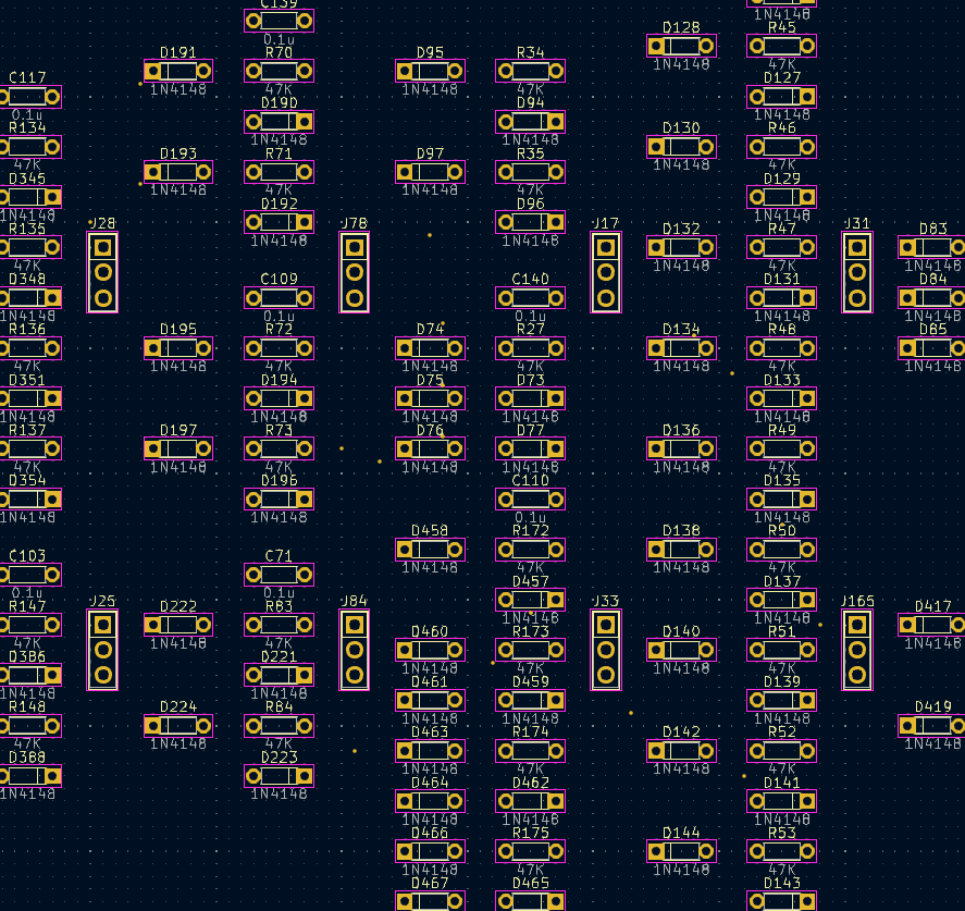
One thing is the tubes are listed by a J number, indicating a connector on the big crystal rectifier circuit board. It connects to one of the 8-tube boards plugged in the back of the crystal rectifier circuit board. So how do we tell what tube is that? For the example J17, it indicates tube 4L-U7B. That means 4th 8-tube board in the left column, and U7B (third tube of bottom row) of that 8-tube board.
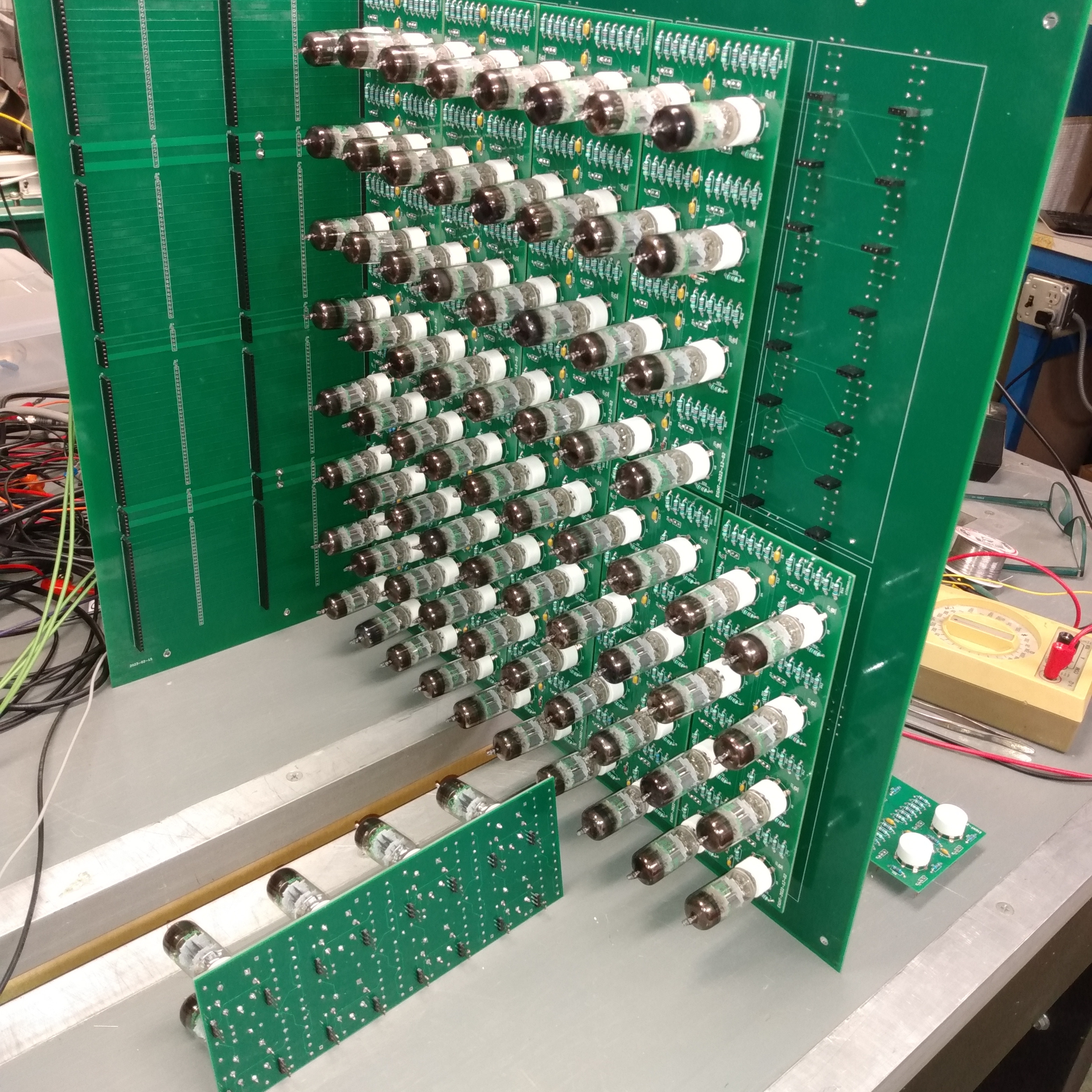 |
| SEQ board on its side with two columns of 8-tube boards. The left column has all 5 8-tube boards, the right column has 5R removed. The 16 Js (2 per tube) are visible where the 8-tube board is removed. |
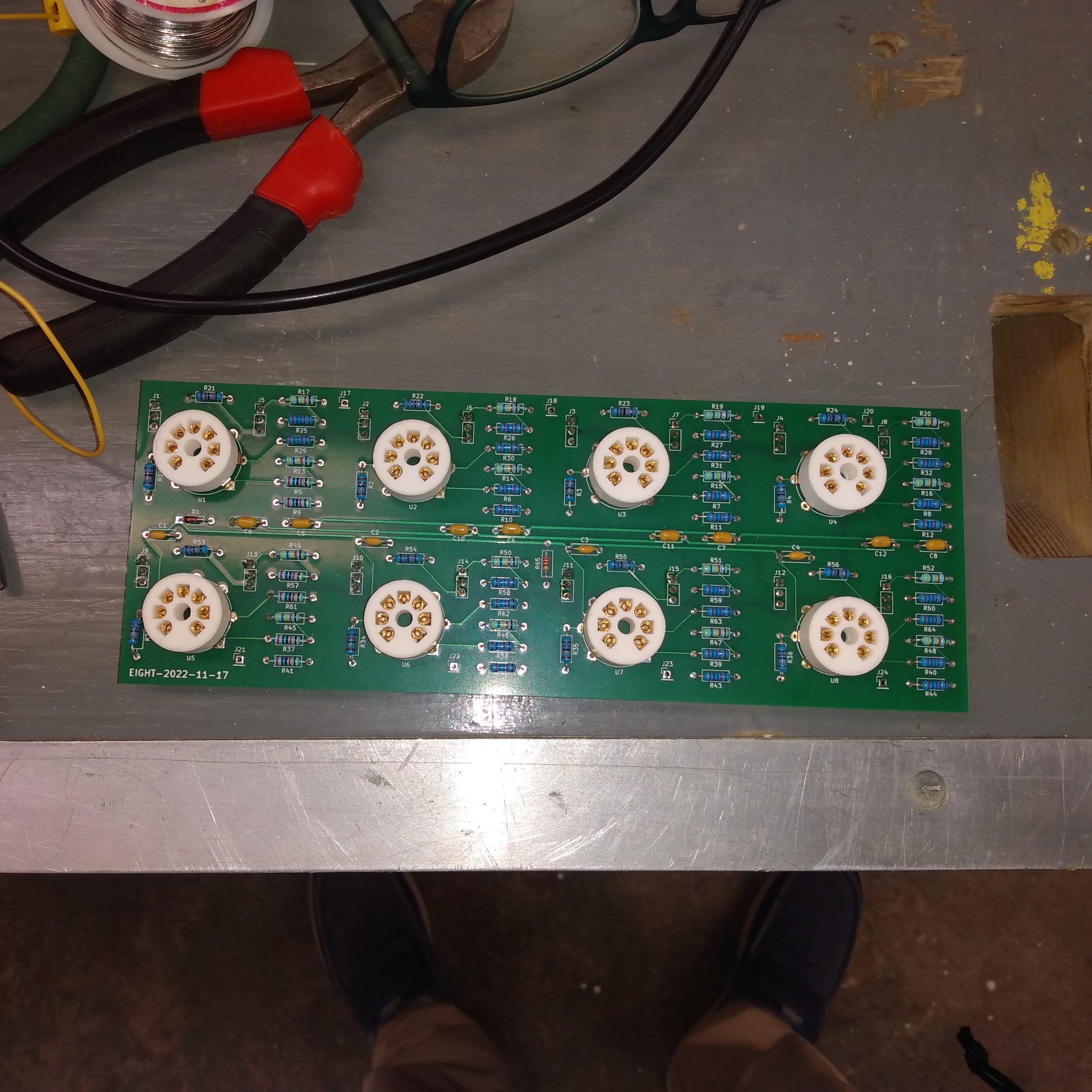 |
| 8-tube board showing U1,U2,U3,U4 on top row, U5,U6,U7,U8 on bottom row. |
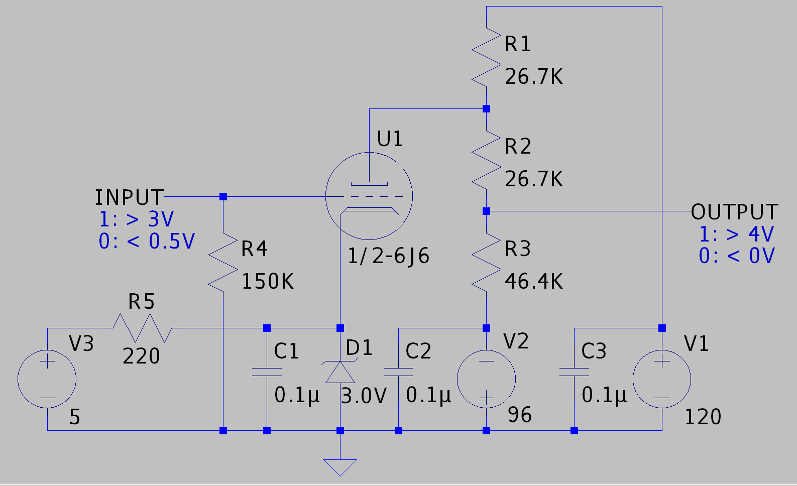 |
| Schematic for one of the 16 sections of the 8-tube boards. Each tube contains 2 triodes. Plate voltage is 60V for one, 40V for zero. |
| KiCad schematic for the whole board. |
The source code is available on GitHub
A Raspberry PI is used to provide memory and peripherals for the processor. It also provides the clock and reset signals. There is a connector on the front panel board that the RasPI plugs into, it could be thought of as the processor's memory and I/O bus.
There is a program that runs on the RasPI called raspictl that uses the GPIO connector to provide needed signals to the bus. It can read in a PDP-8 style .bin file into its memory, start clocking the tubes and provide access to the memory and emulated I/O devices.
The raspictl program also contains a shadow module that knows what the tubes should be doing, cycle by cycle. So the raspictl program knows what the tubes should be placing on the GPIO pins each cycle. It uses that information to verify the signals at the end of each cycle, aborting if there is a mismatch.
The raspictl program can also be used to test the processor by generating random memory contents (opcodes and data) and verifying that the tubes process them correctly. It also randomly generates interrupt requests and verifies the correct response.
For more detailed testing, there are paddles that plug into the 124-line backplane bus that interconnects the boards. They connect to the USB connector on the RasPI and the raspictl program verifies all the bus signals at the end of each clock cycle. Unfortunately the paddles are slow so the processor can only run at 100 cps or so when checking the paddles.
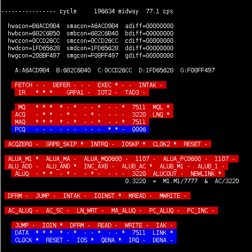
The paddles can also be used to unit test the individual boards. There is a program called autoboardtest that can test individual boards plugged into the paddles, or an arbitrary set of boards plugged into the backplane. The autoboard test program generates random opcodes and data, generates signals for missing boards. It sends them to the connected boards via the paddles, then reads the resulting outputs from the boards via the paddles. Since it uses the paddles, it operates at approximately 100 cps. Example output:
 |
|
The raspictl program can also be run on a PC running Linux by simulating the processor. Passing -csrclib tells it to use a C-equivalent of the processor, automatically generated from the .mod module files. This provides for testing of the module files before making the circuit boards.
The raspictl and autoboardtest programs can also be run on a Zturn Zynq board instead of a Raspberry PI. The .mod files are converted to Verilog then programmed into the FPGA part of the Zynq and the -zynqlib option is passed to either program. The Zynq FPGA code somewhat simulates the speed of the tubes, clocking around 20 kcps. This can be used to test the .mod module files before making circuit boards.
A final option, -pipelib, is available on raspictl and autoboardtest. It uses a TCL-based simulator that accesses the .mod files for simulation and validation, but is very slow (40 cps).
    autoboardtest        csrclib  -  c++ based simulator
    raspictl             physlib  - GPIO connector - the tubes
                         pipelib  - TCL-based simulator
                         zynqlib  -  zynq fpga simulator
On another note, I wrote a Scheme interpreter. It has booleans, 24-bit integers, lambdas, lists, strings. The list of built-in functions is at the very end of that source file. It uses about 6 KW for the code and 2 KW for stack. That leaves 24 KW for source code tokens and heap memory. There are a couple example programs:
The interpreter can be started with the tubes.sh script. When it prompts, enter a command such as (load "test.scm") to run the test program. Or if you want to run the test.scm program on a PC via the simulator, use the test.sh script.
The above mentioned raspictl runs in the Raspberry PI to control the tubes. It can simply load-and-run a bin or rim file if the program just uses the console tty. For example, the Scheme interpreter:
$ ./raspictl scheme.oct
If the program wants to use other devices, raspictl must be started in script mode to define what devices are wanted. It is a TCL interpreter so can actually be programmed. But it also can be used to simply define device parameters. For example, to boot and run OS/8 from an emulated RK8JE:
        $ ./raspictl -script rk8jeboot.tcl

    ...and rk8jeboot.tcl contains:

        loadlink rk8jeboot.oct                  ;# load OS/8 boot program in memory
        reset 0023                              ;# reset processor; set pc = 0023
        option set os8zap 1                     ;# enable OS/8 zap option
        swreg 0                                 ;# set switchregister to 0
        iodev tty telnet 12303                  ;# put tty on telnet port 12303
        iodev rk8je loadro 0 multos8.rk05       ;# load drive 0 file read-only
        iodev rk8je loadrw 1 multos8.rk05.copy  ;# load drive 1 file read/write
        run                                     ;# start clocking the tubes
When those commands complete, the tubes will be clocking away. You will also get a raspictl> prompt. You can enter an exit command when you are done using OS/8, causing raspictl to exit. There are many other commands to control the tubes, enter help to see what they are.
If you don't happen to have the tubes available, the above raspictl commands can take the -csrclib option to use the PC simulator:
        $ ./raspictl -csrclib scheme.oct
        $ ./raspictl -csrclib -script rk8jeboot.tcl
Or you can use -zynqlib if you're running on a Zynq processor programmed with the PDP-8/V code.